MAG*I*CAL® Calibration Standard


|
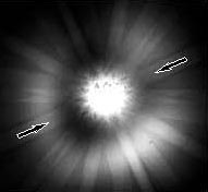
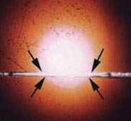
Kikuchi pattern of single crystal silicon viewed down the <011> zone axis. The broad band in the center of this figure is between the [200] Kikuchi lines. |
This standard is directly traceable to the crystal lattice constant of silicon and performs all major instrument calibrations for Transmission Electron Microscopy:
MAG*I*CAL consists of an electron transparent cross-sectional TEM sample made from a MBE grown, single-crystal semiconductor wafer. When the calibration structure is viewed in a TEM, it appears as a series of light and dark layers where the layer thicknesses are accurately known. |
|
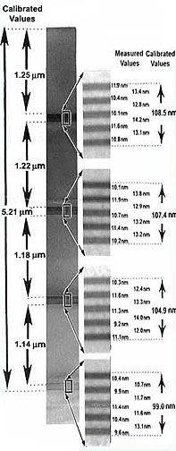
Layer Thickness Values
Calibrated Values = +/- 1.4%
Surface To improve accuracy when making measurements, always measure the largest distance clearly visible on the micrograph. For example, at the highest magnification ranges, measure the distance across the entire set of five dark layers and four light layers, instead of trying to measure an individual dark layer. |
|
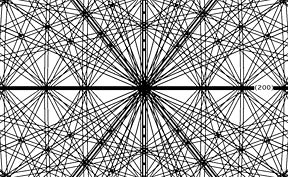
Diagram of the MAG*I*CAL® grid. The arrows point to the four regions containing the calibration marks. |
|
A Kikuchi pattern from the single crystal sample which can be used to align the sample. | |
|
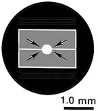
An optical micrograph of the colors of silicon when it is thinned down to TEM thicknesses, the 1mm central perforation, and the four areas containing the calibration markings (arrows). | |

|
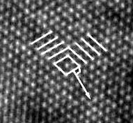
A lattice image of the single crystal silicon sample. The silicon <1 1 1> lattice planes should be measured perpendicular to the planes, in the direction of the arrow. |
| Prod # | Description | Unit |
|---|---|---|
| 675 | MAG*I*CAL® Calibration Standard | each |
专业代理国外知名镊子品牌
我们将竭诚为你服务
0755-23003036