
I101 perovskite ink has been specially formulated in the Ossila laboratories to be deposited by spin coating. Our I101 perovskite ink is designed for air processing in low-humidity environments. Using a mixture of methyl ammonium iodide (MAI) and lead chloride (PbCl2) dissolved in dimethyl formamide, our I101 perovskite ink will convert to a methylammonium lead halide perovskite under heat. The final product is a methylammonium lead iodide perovskite with trace amounts of chlorine given by the formula CH3NH3PbI3-xClx.
The main use of CH3NH3PbI3-xClx is in the fabrication of solar cells, our I101 ink can be used in both standard and inverted architectures; and can achieve power conversion efficiency (PCE) values of over 13% (see our device performance section for more information).
Using our I101 recipe provided, 5ml of solution is capable of processing up to 160 substrates (1,280 devices using our 8-pixel substrate design).
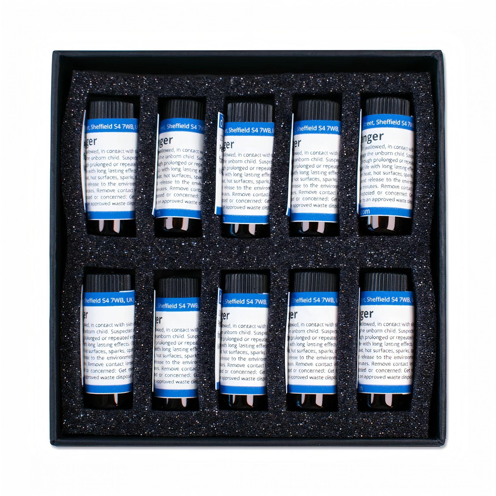
I101 is packaged as 10 individual vials containing 0.5 ml of solution capable of coating up to 160 substrates. I101 can also be bought in bulk (30 ml) with a 25% discount over our standard order sizes.
| Perovskite Type | CH3NH3PbI3-xClx |
|---|---|
| Precursor Materials | Methyl Ammonium Iodide (99.9%), Lead Chloride (99.999%) |
| Precursor Ratio | 3:1 |
| Solvent | Dimethyl Formamide (99.8%) |
| Optical Bandgap | 1.56 – 1.59 eV |
| Energy Levels | Valence Band Minimum 5.4 eV, Conduction Band Minimum 3.9 eV |
| Emission Peak | 770 – 780 nm (PL); 755 – 770 nm (EL) |
| Standard Architecture PCE | 13.7% Peak; 13.0% ±0.25% Average |
| Inverted Architecture PCE | 13.1% Peak; 11.9% ±0.50% Average |
| Processing Conditions | Air processing; low humidity (20% to 35%) |
| Packaging | 10 x 0.5 ml sealed amber vials; 3 x 10 ml sealed amber vials |
Below is information on photovoltaic devices fabricated using our standard architecture and inverted architecture recipes for I101 inks. All scans were taken after 10 minutes under illumination of an AM1.5 source, using a voltage sweep from -1.2 V to 1.2 V then from 1.2 V to -1.2 V at a rate of 0.2 V.s-1; no bias soaking was performed on devices.
| Architecture | Standard | Inverted | ||
|---|---|---|---|---|
| Sweep Direction | Forward | Reverse | Forward | Reverse |
| Power Conversion Efficiency (%) | 13.5 | 13.7 | 12.4 | 13.1 |
| Short Circuit Current (mA.cm-2) | -20.8 | -20.8 | -18.8 | -18.8 |
| Open Circuit Voltage (V) | 0.88 | 0.90 | 0.96 | 0.96 |
| Fill Factor (%) | 73 | 73 | 69 | 72 |
 JV curve under AM1.5 irradiation for a standard (left, courtesy of Michael Stringer-Wong, University of Sheffield) and inverted (right, courtesy of Alex Barrows, University of Sheffield) device based on Ossila's I101 ink. Device characteristics were recorded on a reverse sweep.
专业代理国外知名镊子品牌
我们将竭诚为你服务
0755-23003036