Triple Cation Perovskite Precursor Ink (for Nitrogen Processing)


I301 perovskite ink has been formulated in conjunction with our research partners to obtain the highest possible PCEs. Our I301 perovskite ink is designed for processing inside controlled environments such as a nitrogen-filled glove box.
Ossila’s I301 contains a formulation of Methylammonium Bromide (MABr), Lead Bromide (PbBr2), Formamidinium Iodide (FAI), Lead Iodide (PbI2) and Caesium Iodide (CsI) in DMSO solvent. After undergoing conversion through a combination of solvent quenching and thermal annealing steps, I301 ink can be used to create a (Cs0.05FA0.81MA0.14)Pb(I0.85Br0.15)3 perovskite film. For information on the various application of this mixed-cation perovskite, see our applications section.
The main use of I301 is in the fabrication of solar cells. The process recipe for I301 is optimised for glove box processing under a nitrogen atmosphere. This ink is designed to be used with the device architecture ITO-coated glass/SnO2/perovskite/Spiro-OMeTAD/Au. PV devices using this architecture achieved an average / peak power conversion efficiency (PCE) of (16.4% ± 3.9)% / 19.0%. (see our device performance section for more information). The ink specifications can be found below along with complete guides on the processing of perovskite inks for standard architecture. Using our provided I301 recipe, 5 ml of solution is capable of processing up to 100 substrates (800 devices using our 8-pixel substrate design).
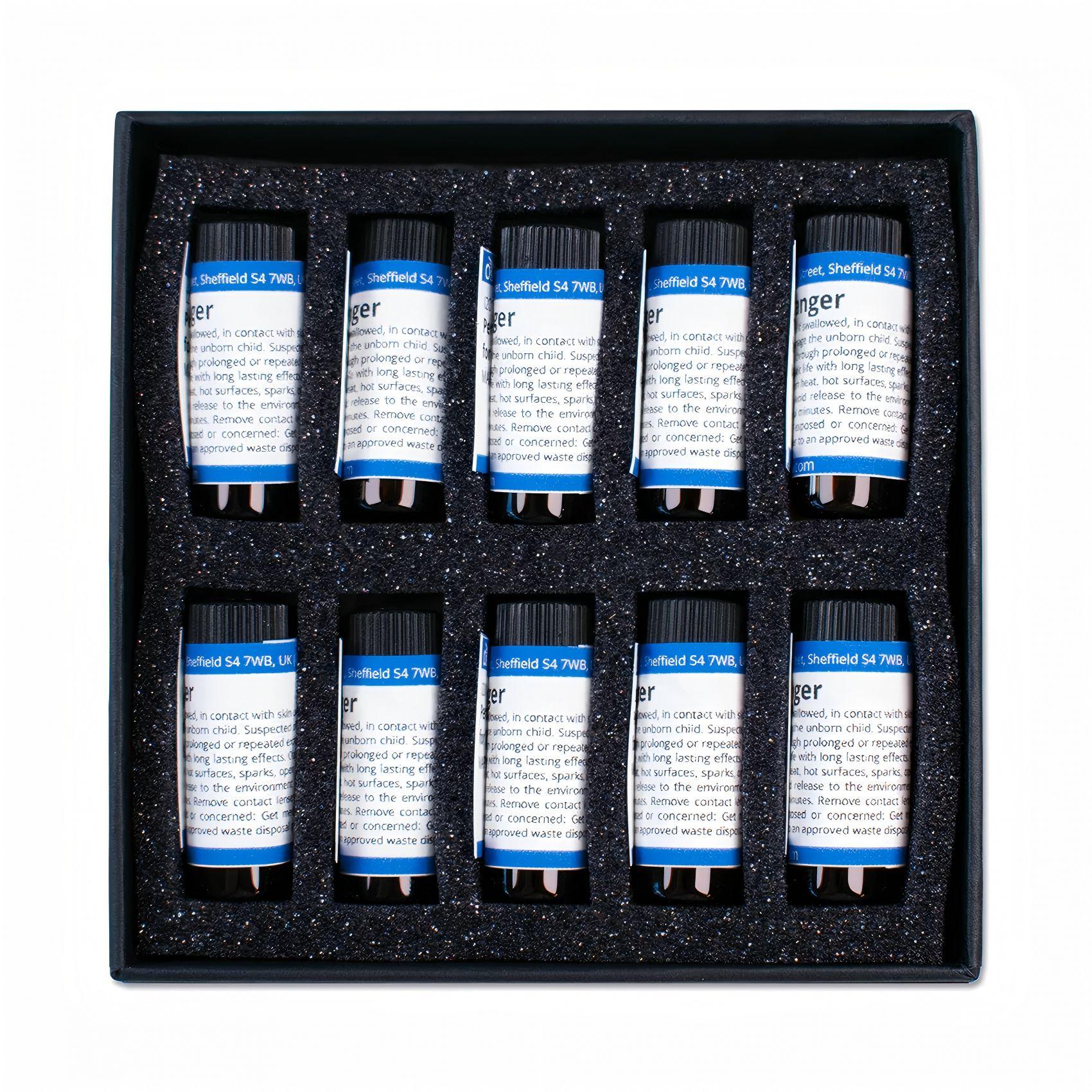
 I301 is packaged as 10 individual vials containing 0.5 ml of solution each, capable of coating up to 100 substrates.
| Perovskite type | (Cs0.05FA0.81MA0.14)Pb(I0.85Br0.15)3 |
|---|---|
| Precursor materials (purity) | Formamidinium iodide (98%), lead iodide (99.999%), methyl ammonium bromide (98%), lead bromide (99.999%), Caesium Iodide |
| Precursor ratio | 1.00 : 1.05 : 0.18 : 0.19 : 0.06 |
| Solvent (purity) | Dimethyl sulfoxide (99.8%) |
| Optical bandgap | 1.5-1.6 eV |
| Emission peak | 787 nm |
| Standard architecture PCE | 19.0% Peak; 16.4% ± 3.9% Average |
| Processing conditions | Inert environment only (e.g. nitrogen or argon atmosphere) |
| Packaging | 10 x 0.5 ml sealed amber vials |
| Storage Conditions | Must be kept refrigerated. Only open in an inert atmosphere. |
Perovskite Photovoltaics: Multiple cation inks are used to create high efficiency devices, regularly achieving over 20% (see the papers cited below). Double cation inks contain two organic A-cations: methylammonium (CH3NH3+,MA) and formamidinium (CH3(NH2)2+,FA). Double cation perovskites produce impressive initial PCEs but have thermal and phase instabilities, due to the volatility of MA and the phase instability at room temperature of FA-based perovskites. By adding a small amount of Caesium to the precursor, high efficiency devices of 21.1% can maintain over 80% of their initial efficiency after 250 hours of device aging. Below are a series of papers studying multiple cation perovskite inks.
The formulation of triple cation inks varies amongst the literature. Researchers working with Ossila have optimised the I301 ink to produce a high performance ink with impressive lifetime in solution.
Below is information on photovoltaic devices fabricated using our standard architecture recipe for I301 inks. All scans were taken under AM1.5 illumination, sweeping the voltage from -0.2 V to 1.2 V then from 1.2 V to -0.2 V at a rate of 0.2 V.s-1 ; no bias soaking was performed on devices.
Best Device Performance| Sweep direction | Forward | Reverse |
|---|---|---|
| Power conversion efficiency (%) | 19.3 | 18.9 |
| Short circuit current (mA.cm-2) | -22.4 | -22.3 |
| Open circuit voltage (V) | 1.08 | 1.09 |
| Fill factor (%) | 79.7 | 77.8 |
| Power conversion efficiency (%) | 16.4 ± 3.9 |
|---|---|
| Short circuit current (mA.cm-2) | -21.2 ± 0.9 |
| Open circuit voltage (V) | 1.01 ± 0.20 |
| Fill factor (%) | 73.9 ± 11.9 |
 JV sweep for Best Performing Device
 Stabilised PCE for Best Performing Device
专业代理国外知名镊子品牌
我们将竭诚为你服务
0755-23003036