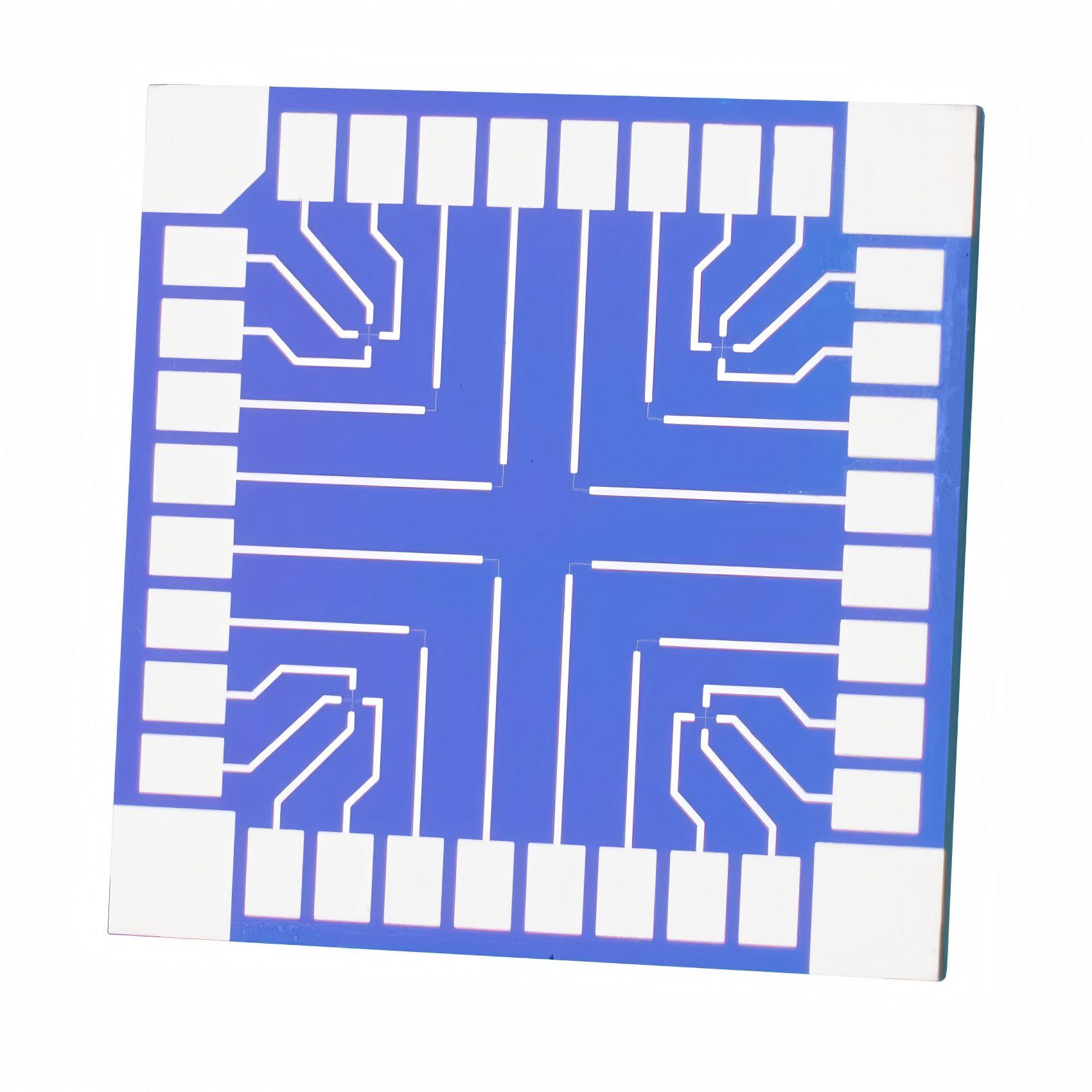
Platinum FET Test Chips, Optimized for 2D Materials


Ossila’s 2D material FET test chip is designed to allow users to perform electrical and optical measurements on monolayer or few-layer 2-dimensional (2D) crystals, without the need for expensive lithography equipment. Our chips come prepatterned with platinum electrodes on a Si-SiO2 substrate, with source-drain channel lengths ranging from 4 µm to 20 µm. Transfer your crystal across the channel and you are ready to measure. The chips also feature dual channel electrodes that allow you to stack two crystals on top of each other and contact each separately.
Research into 2D materials has been steadily growing in popularity for several years, fuelled by the promise of revolutionary new technology in areas ranging from batteries to quantum computers. The preferred method for 2D material preparation (within the research community at least) is the so-called 'Scotch-tape' method, where monolayer or few-layer crystals are peeled from bulk material. This method currently gives the highest quality 2D materials needed for optical and electronic applications. The preparation of 2D materials in this way is relatively straightforward, and optical measurements can require little more than a microscope and a light source.
However, to reach their full potential, the electrical characteristics of 2D materials needs to be studied. This posses a large barrier to entry for the researcher, as complicated and expensive lithography equipment is required to create the electrical contacts to the 2D crystals. We have developed our 2D material FET substrates in partnership with researchers in the field to remove this barrier, and to speed up the electrical and optical characterisation of 2D materials.
| Substrate / Gate | Silicon (n-doped) |
| Gate resistivity | ~5 Ωcm |
| Gate dielectric | 300 nm thermally grown silicon dioxide |
| Dimensions | 14.97 mm x 14.97 mm x 0.7 mm |
| Electrode pad pitch | 1.27 mm |
| Electrode width | 4 µm |
| Electrode material | Platinum (50 nm ± 10 nm) / Titanium adhesion layer (5 nm) |
| Deposition method | Plasma sputtering |
| Patterning method | Photolithography |
| Channel lengths |
4 µm (2x) 10 µm (2x) 4 µm x 10 µm 4 µm x 20 µm 10 µm x 20 µm 10 µm x 20 µm variable length (x4) |
专业代理国外知名镊子品牌
我们将竭诚为你服务
0755-23003036