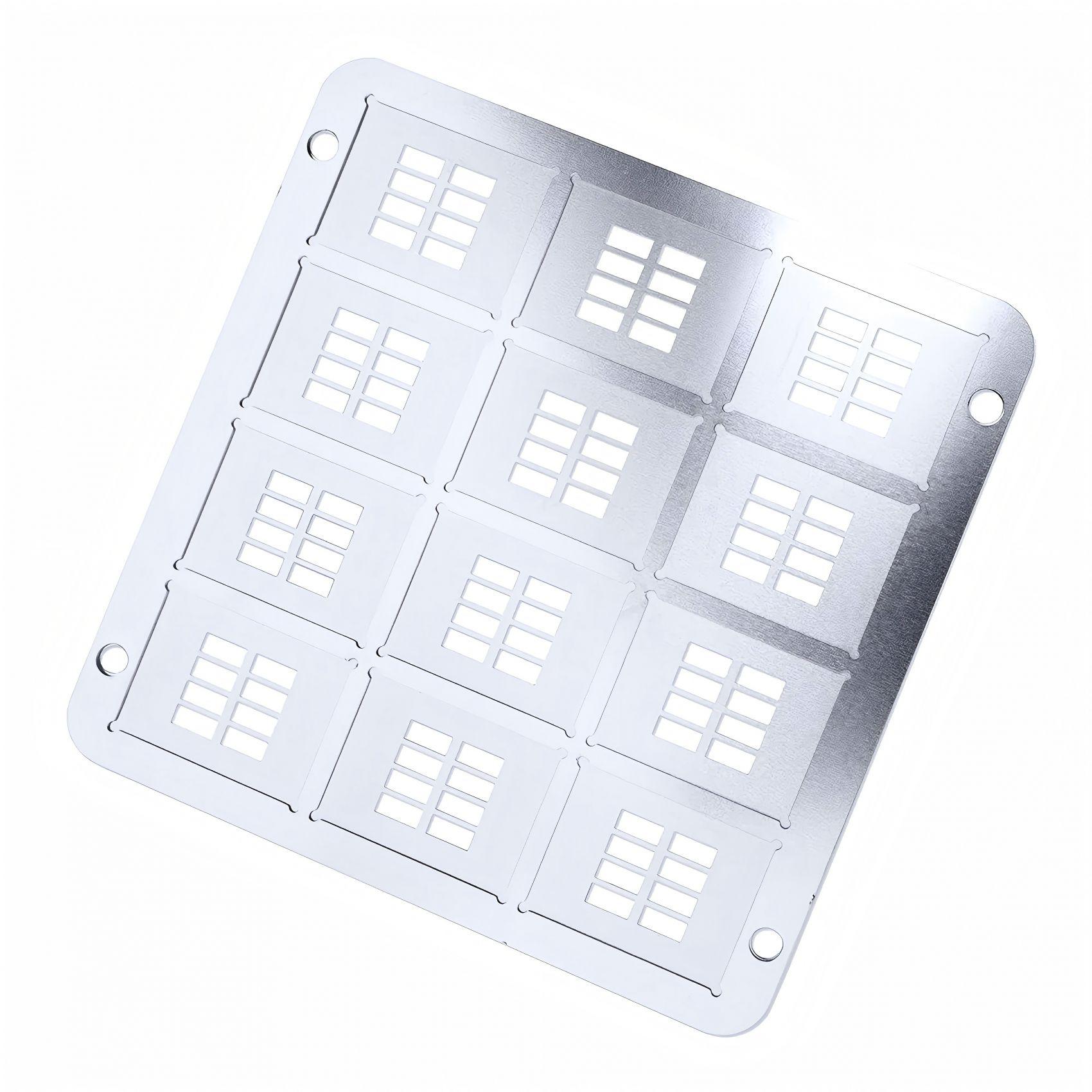
Deposition Masks, 20 x 15 mm


Ossila have produced a range of masks for vacuum deposition of materials onto our standardised 8-pixel substrate design. These include masks that are used to deposit electrodes and busbars and masks to deposit semiconducting materials to define an active area for thin film electronic devices - all to obtain the highest device performances possible. All our deposition masks are made from stainless steel, with the option of an additional spacer layer.
Looking for generation I (E114/5/6, E631) or II (E345/6, E355/6) deposition masks for S101 or S171 substrates?
We have discontinued our generation I and generation II substrates and masks. The replacement 8-pixel design allows you to create either eight small individual pixels or a single large pixel. Contact us for more information, technical support and advice, or for help migrating to the new system.
We provide the following masks that are suitable for use with our S211 substrate design:
Each mask has the option of the addition of a 100 µm spacer layer that can be placed between the mask and the substrate. This spacer layer reduces the direct contact between the surface of the substrate and the mask by over 98%. This is recommended for samples that are easily scratched or for porous samples that experience a large amount of out-gassing. For sputtering or other non-directional deposition techniques, the spacer layer is not recommended as the presence of a spacer layer will reduce the precision of your deposited edge.
| Material | Stainless Steel |
| Outer Dimensions | 75mm x 75mm |
| Substrate Recesses | 12 |
| Recess Dimensions | 20.15mm x 15.15mm |
| Thickness | 1.7mm without spacer, 1.8mm with spacer (E504: 1.6mm without spacer, 1.7mm with spacer)(exc. bolts) |
专业代理国外知名镊子品牌
我们将竭诚为你服务
0755-23003036