General Information
|
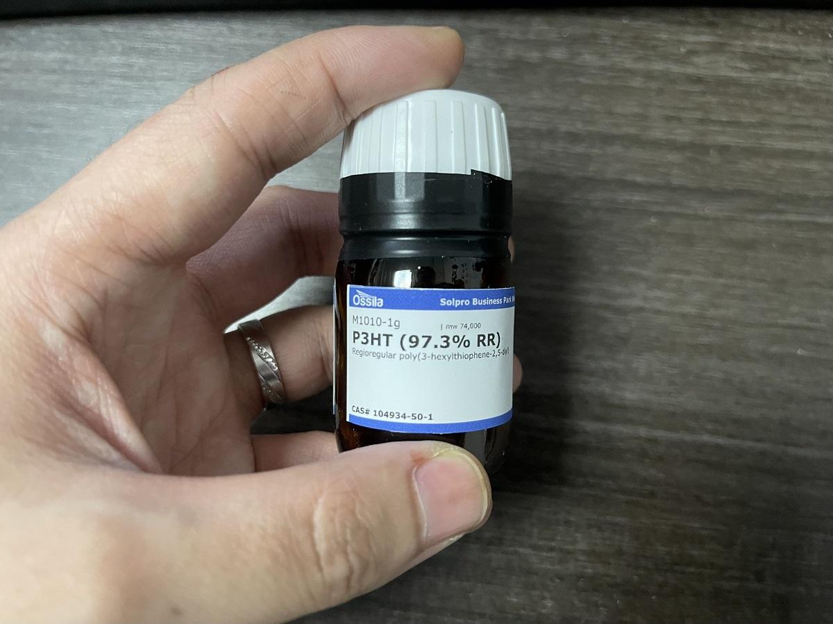
Full name
|
Poly(3-hexylthiophene-2,5-diyl)
|
|
Synonyms
|
P3HT
|
|
CAS number
|
104934-50-1
|
|
Chemical formula
|
(C10H14S)n
|
|
Molecular weight
|
See the Batch Details table at bottom of the page for information
|
|
HOMO / LUMO
|
HOMO = -5.2 eV, LUMO = -3.2 eV
|
|
Solubility
|
Chloroform, chlorobenzene
|
|
Classification / Family
|
Polythiophenes, Organic semiconducting materials, Low band gap polymers, Polymer donors, Organic photovoltaics, Polymer solar cells, OLEDs, OFETs
|
OFET Fabrication Routine
This procedure details the fabrication and charge mobility measurements for OFETs made from the M104 batch of P3HT. Download a full OFET fabrication report.
Field effect mobilities in excess of 0.12 cm2/Vs are recorded using M104 when the active layer is dispensed on OTS-treated silicon oxide dielectric by static spin coating from an optimized high/low boiling point solvent mix.
High hole mobility in conjunction with good solubility and partial air stability make regioregular P3HT a reference material of choice for both fundamental and applied research in organic electronic, physics and chemistry. As one of the most well-studied organic semiconductor, P3HT is often acknowledge to be one of the benchmark against which any new p-type or donor conjugate molecule should be compared and evaluated.
Mobility has previously been found to be positively correlated with increasing region-regularity, slow drying time (achieved using high boiling point solvent), lowering of the surface energy, and molecular weight in excess of 50 kD. These conditions favour p-p stacking parallels to the OFET substrate, which in turn results in improved charge transport across the transistor channel [1-13].
|
Substrate size
|
20 x 15 mm
|
|
Gate conductivity
|
1-30 O·cm (Boron doped)
|
|
Silicon oxide thickness
|
300 nm
|
|
Device per substrates
|
Five, common gate
|
|
Channel length
|
30 µm
|
|
Channel width
|
1000 µm
|
The active layer solution preparation, spin coating, substrate annealing and measurements are performed in a glove box under a nitrogen atmosphere (H2O <0.1 PPM; O2 < 5/8 PPM).
For generic details on the fabrication of OPV devices, please see our written guide and video demonstration.
Active Layer Preparation
High-Regioregular and high molecular weight RR-P3HT (M104) (RR = 96.3%, Mw = 77,500, Mn = 38,700) is dissolved in a mix of high and low boiling point solvent in order to exploit the beneficial effect of long drying time and increase the wettability of low energy surface, respectively.
-
5 mg/ml of M104 dissolved in anhydrous Chloroform:Trichlorobenzene (99:1) mix;
-
Vial is placed on hot plate (70°C) with a stirrer bar for 30 minutes;
-
Solution cooled down at room temperature and then filtered with a 0.45 µm PTFE (hydrophobic) filter;
-
Solution stored overnight on a hot plate at 30°C to prevent excessive aggregation of the P3HT molecules.
Substrate Cleaning
-
Substrates loaded on to substrate rack (to keep them in upright position);
-
Sonicated in hot Hellmanex III solution (1%) for five minutes;
-
Rinsed twice in hot water;
-
Sonicated in warm Isopropyl alcohol (70°C) for five minutes;
-
Rinsed twice in cold DI water;
-
Substrates stored in DI water.
Thermal Deposition of Electrodes and Contact Pads
-
Done on Edwards 306 Thermal coater in clean room condition;
-
Substrates are blown dry and loaded in a low density evaporation stack with a low density shadow mask to pattern the desired features;
-
Secondary mask is added to selectively evaporate the gate and drain/source pads;
-
Vacuum chamber pumped down to a vacuum pressure of 5 x 10⁻⁶ mbar;
-
Chromium adhesion layer: 5 nm, rate 0.05 nm/s;
-
Aluminum: 80 nm, rate: 0.4 nm/s;
-
Changed secondary mask to deposit electrodes (FET channels);
-
Vacuum: 2-3 x 10⁻⁶ mbar;
-
Chromium adhesion layer: 1 nm, rate 0.05 nm/s;
-
Gold: 40 nm; rate 0.05 nm/s.
PFBT Treatment for Au Electrodes (Laminar flow)
-
Oxygen plasma treatment, 30 seconds at 100 W;
-
Substrates immersed in 2.5 mMol/l solution of PFBT in isopropyl alcohol at room temperature;
-
Substrates rinsed twice in pure isopropyl alcohol;
-
Substrates are blown with nitrogen gun.
OTS Treatment for SiO2 Dielectric (Laminar flow)
-
A solution of OTS (25 microlitres) in cyclohexane (anhydrous grade, 1 ml) prepared in glove box;
-
Substrates (pre-loaded on a substrate rack) loaded into the annealing beaker, which is filled with approx. 50 ml of cyclohexane in a fume hood;
-
Previously prepared OTS solution quickly added to the cyclohexane and mixed with a pipette tip;
-
The glass lid is placed halfway onto the beaker, which is carefully filled with more cyclohexane until it is full and the lid is fully closed;
-
The final solution (60 ml) contains OTS at a concentration of 1 mMol/l;
-
Substrates kept for 20 minutes in the OTS solution;
-
Substrates removed from the OTS solution, quickly rinsed twice in clean cyclohexane, and then are blown dry with nitrogen gun.
Contact Angle Assessment
The water-drop test on the treated silicon is a quick test to qualitatively assess the effect of the OTS on the silicon substrates to ensure that the fabrication has functioned correctly. You can get a good approximation of the contact angle using your eye or a simple digital photo.
Previous quantitative assessments have shown that this routine will produce contact angles between 90 and 110°C (depending on the lab temperature, humidity and other factors). You can quantify that contact angle easily and accurately using the Ossila Contact Angle Goniometer.
P3HT (M104) spin coating (glove box)
-
30 µl of Organic Semi-Conductor (OSC) solution delivered on the middle of the substrate and then spin coated at 1000 rpm for 10 s followed by 60 s at 2000 rpm;
-
Cotton swab soaked in chlorobenzene to thoroughly wipe clean the contact pads and the rest of the substrates with the exception of the area around the channel;
-
High precision cotton swab to clean between devices to avoid cross-talking and reduce leakage;
-
Substrates annealed at 90°C for 30 minutes;
-
Cooled down for ten minutes;
-
Five devices per substrate are characterised using OFET Test Board for Low-Density OFETs in a glove box;
-
Second annealing at 120°C for 20 minutes, slow cooling down at room temperature and measurement;
-
Annealing at 150°C for 20 minutes, slow cooling down at room temperature and measurement.