Hole Transport Layer Materials, Interface Polymers, Luminosyn™ Polymers, Materials, OFET & OLED Poly


PCDTBT (CAS number 958261-50-2) is one of the next generation donor materials developed for organic photovoltaics to produce better efficiencies and lifetimes. The key properties of PCDTBT result from the lower HOMO/LUMO levels which lead to advantages over standard organic photovoltaic materials of increased open circuit voltage, longer wavelength absorption and improved stability under ambient conditions.
The lower lying HOMO level of PCDTBT makes it much more stable under ambient conditions and therefore an ideal candidate to use with large area deposition methods such as ink-jet printing, spray coating and blade coating. However, for these deposition techniques, uniform, aggregate free coatings are essential and so lower molecular weights are often desirable.
| CAS Number | 958261-50-2 |
|---|---|
| Chemical Formula | (C43H47N3S3)n |
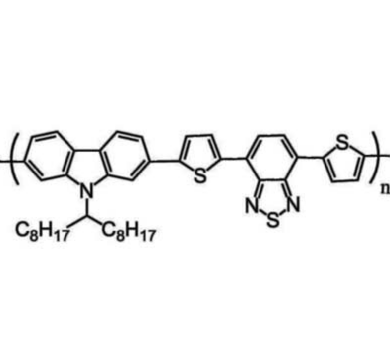
| Full Name | Poly[N-9'-heptadecanyl-2,7-carbazole-alt-5,5-(4',7'-di-2-thienyl-2',1',3'-benzothiadiazole)] |
| Molecular Weight | See Batch Details for information |
| HOMO / LUMO | HOMO = -5.4 eV, LUMO = -3.6 eV |
| Solubility | Chloroform, chlorobenzene, dichlorobenzene and trichlorobenzene |
| Synonyms | PCDTBT |
| Classification / Family | Polycarbazoles, Heterocyclic five-membered ring, Organic semiconducting materials, Low band gap polymers, Organic photovoltaics, Polymer solar cells, OLEDs, OFETs and Perovskite solar cells |
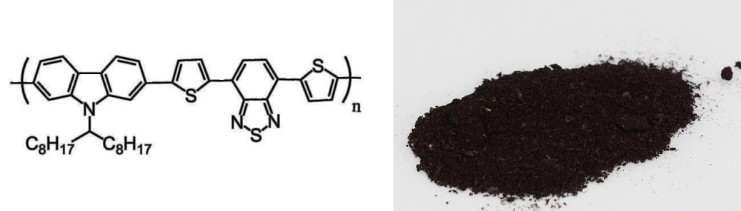 Chemical structure of PCDTBT
For high performance organic photovoltaics with efficiencies of 6% and above poly[N-9'-heptadecanyl-2,7-carbazole-alt-5,5-(4',7'-di-2-thienyl-2',1',3'-benzothiadiazole)] (PCDTBT). We have achieved efficiencies of 6.7% in our own labs using a standard reference architecture of PEDOT:PSS as a hole interface and calcium/aluminum as an electron interface (see below for fabrication details). Our paper published in Nature Scientific Reports titled Molecular weight dependent vertical composition profiles of PCDTBT:PC71BM blends for organic photovoltaics explores the effect and optimisation of molecular weight.
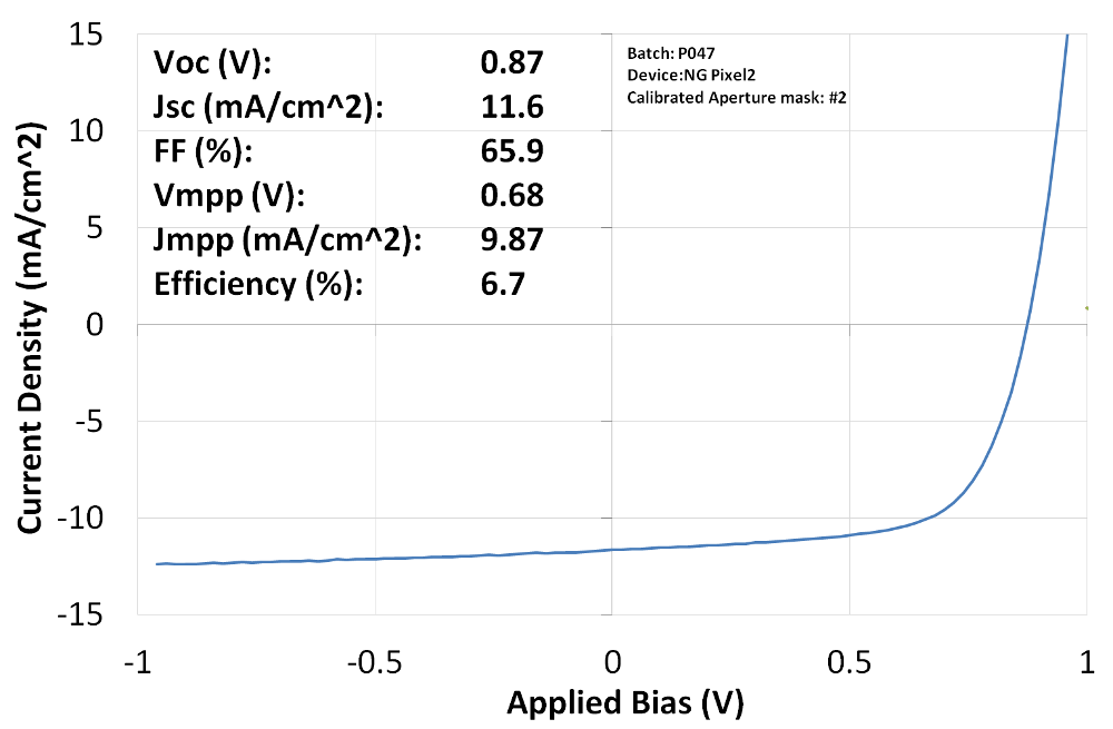 JV curve from PCDTBT in a standard reference device. HOMO/LUMO = -5.4 eV / -3.6 eV, Bandgap = 1.8 eV; CAS number 958261-50-2
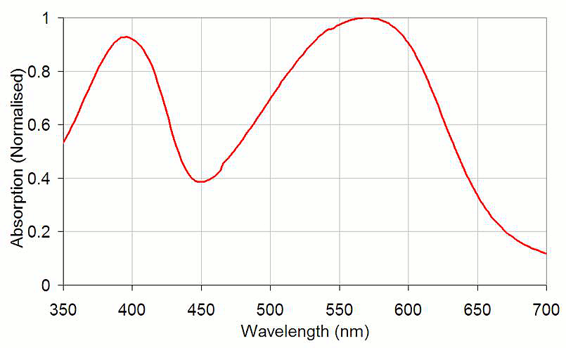 PCDTBT UV-Vis Absorption Spectrum
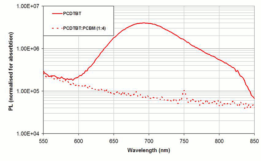 PCDTBT Photoluminescence Spectrum
Ossila’s reference devices were made by dissolving PCDTBT at 4 mg/ml in anhydrous chlorobenzene using a stir-bar and hotplate at 80°C overnight. This was then mixed with Ossila’s dry 95%/5% C70-PCBM powder in a 1:4 blend ratio to produce an overall concentration of 20 mg/ml. The blend solution was heated with a stir-bar on a hotplate at 80 °C for 2 hours before cooling to room temperature over 10 minutes and filtering with a 0.45 μm PTFE filter immediately prior to spinning at 700 rpm to give a film of approx. 70 nm.
Glass / ITO / PEDOT:PSS / PCDTBT:PC70BM / Ca / Al
Ossila’s pre-patterned ITO substrates (S211) with 100 nm (20 Ω/square) ITO were cleaned with the following procedure:
PEDOT:PSS AI 4083 was filtered through a 0.45 µm PES filter (C2009S1) before spin coating at 6000 rpm in air to produce a layer 30 nm thick. The coated substrates were then stored on a hotplate at 150 °C before transfer into a glove box and a further bake of 150 °C for 10 mins to remove any residual moisture. The active ink was spin cast and the cathode strip wiped clean using chlorobenzene before transfer to an evaporator where 2.5 nm of Ca followed by 100 nm of Al were deposited at <10-6 mbar. The substrates were then annealed at 80 °C for 15 mins on a hotplate in the glove box before protecting with the Ossila encapsulation system. Measurement was performed under ambient conditions using a Newport 92251A AM1.5 100 mW/cm2 solar simulator and NREL certified silicon reference cell.
专业代理国外知名镊子品牌
我们将竭诚为你服务
0755-23003036